In writing these articles, I have moved from topics that I am very familiar with, to topics that I know very little about. In other words I am now using the process of writing the articles as a way of learning more about things that I am interested in and want to understand. With luck my knowledge gaps coincide with those of most readers, so we can enjoy the learning experience together! Solar cells are becoming ubiquitous as alternate sources of energy are developed in anticipation of the inevitable decline in hydrocarbon reserves, yet I have had no clue how they work. This month’s article is a brief summary of what I’ve learned about the science behind solar cells.
Digging deep into the memory banks, some of us may recall the photoelectric and photovoltaic effects from physics class. The photoelectric effect is seen when a material gives off electrons when it is exposed to sufficient levels of short wavelength electromagnetic energy. The photoelectric effect does not play a role in this article. The related but different photovoltaic effect, with a confusingly similar name, is central to the topic being discussed. With the photovoltaic effect, electrons are also generated or released from the material being exposed to electromagnetic radiation, but rather than being emitted from the material, they are transferred from one material to another, resulting in a potential difference between the two materials, i.e. a voltage (or the current associated with the voltage). This, obviously, is the physical effect exploited by solar cells. You could think of solar cells as being a subset of the larger, more general field of photovoltaic cells; with the former the energy source is solar radiation, while with the latter the energy source might come from anywhere within the broad spectrum of electro-magnetic radiation.
So, we’ve established that solar cells are devices that produce electricity from solar energy via the photovoltaic effect. How do they actually work, and how are they constructed? To answer those questions in a short and simple way requires an understanding of the fundamental economic drivers at play. Solar cells need to be competitive in a financial sense with traditional hydrocarbon-based methods of generating electricity – typically coal, oil and gas fired power generation plants. With sunlight being free, the cost function is defined by the tradeoff between the cost of producing the solar cell and its efficiency. A tremendous amount of research effort is being devoted to both bringing down the costs to produce solar cells and increasing the efficiency with which they convert sunlight to electricity. This has resulted in a bewildering range of solar cell types, distinguished by materials used, production processes, configurations, implementations, etc., etc. For simplicity’s sake, let’s stick to looking at the most common solar cell in commercial use, thin wafer silicon with a large area p-n junction configuration.
How are p-n junction solar cells constructed?
At the heart of a p-n junction solar cell is a two-sided wafer with a high electron concentration layer on one side made of n-type silicon, and a low electron concentration layer on the other side made of p-type silicon, with an area of diffusion in the middle referred to as the junction. This wafer is a basic type of semi-conductor. Typically the cell is constructed of the following layers, starting at the top side facing the sun:
A layer of glass at the top to separate the silicon from the elements.
Thin metallic strips, called fingers, which supply generated current to larger bus bars.
An anti-reflective coating to maximize absorption.
A layer of n-type silicon, called the emitter.
A layer of p-type silicon, called the base.
The back contact that completes the circuit with the fingers on top.
The top and bottom metallic semiconductor contacts (fingers+buses and back) are connected to the external system that “collects” the electricity generated by the cell. A single solar cell will produce a very small amount of electricity, so in typical configurations solar cells will be arranged in modules with both serial and parallel connections. The voltages from cells connected in series add up, while parallel connections increase current; by combining the two, solar arrays can be configured in a way to produce the desired voltage and current characteristics.
It should be noted that these cells are not simply constructed by sticking n- and p-type silicon wafers together side-by-side. The process is quite complex and expensive, and involves diffusing n-type dopant into one side of a p-type wafer, or vice versa. The boundary between the two layers (the p-n junction), is therefore not a sharp one, but rather a gradual change (at atomic scale) from p- to n-type silicon. Furthermore, there are different types of the bulk silicon used in the wafers, each with its own advantages and disadvantages determined by production cost and efficiency – monocrystalline, multicrystalline and ribbon silicon.
How do p-n junction solar cells work?
When a p-n junction solar cell is exposed to sunlight, some of the light is reflected – an inherent inefficiency. The light photons that aren’t reflected enter the cell, and some are absorbed by the electrons within the silicon wafer’s crystalline
lattice. These electrons are normally held in place by covalent bonds with neighbouring atoms, or in other words they are in the valence band. If the energy of the absorbed photons is high enough to move the electrons out of the valence band into the conduction band, then they are freed from their covalent bonds and are at liberty to move around within the wafer. Each freed electron leaves behind a hole in the covalent bond it has abandoned. This hole represents a spot for a neighbouring electron to move into, which in turn leaves behind a hole. Thus it can be seen that the absorption of photons creates electron-hole pairs which are free to move around within the solar cell independently.
It happens that most of the solar radiation that reaches the Earth’s surface has energy levels that exceed the amount required to move electrons from the valence band into the conduction band (called the band gap) in crystalline silicon. The energy over and above that band gap mostly creates vibrations in the lattice and is converted into heat. This is another area of inherent inefficiency in current silicon solar cells. Energy that is below the band gap mostly passes right through the silicon.
The following sequence of figures describes the physical mechanisms at play within the solar cell.
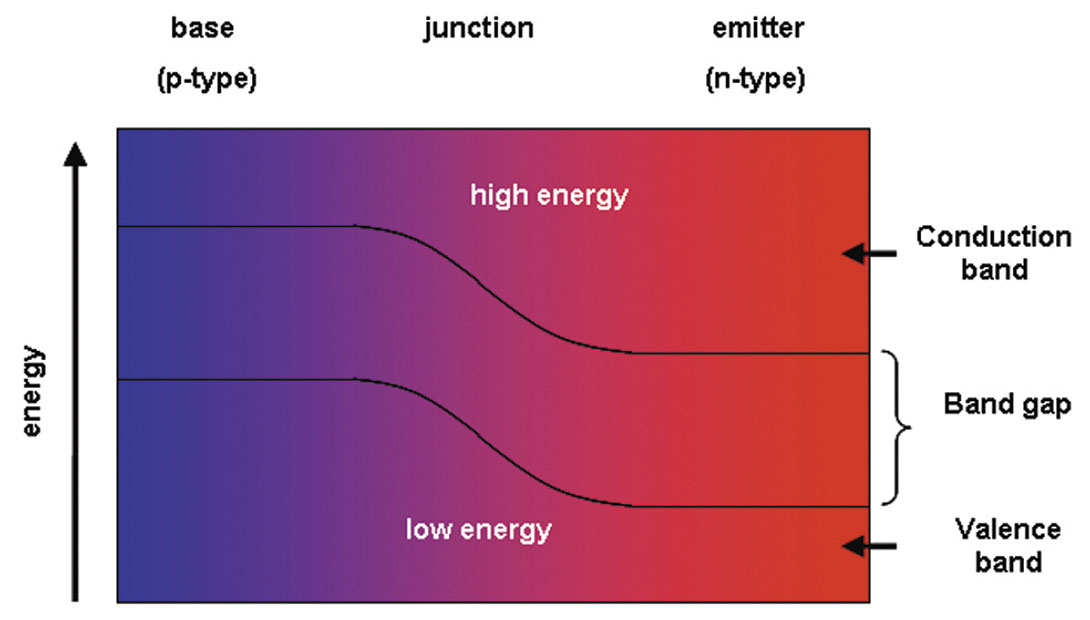
1. This figure shows the solar cell in its non-excited state, i.e. not receiving any sunlight. Note that the (conceptual) vertical axis represents energy level, with the low energy valence band at the bottom, and the high energy conduction band at the top. Take note that these two energy levels are slightly higher within the p-type silicon layer than the n-type layer. The (physical) horizontal axis is a spatial one representing the solar cell’s cross-section, with the sun-facing top of the cell on the right, and the bottom on the left.
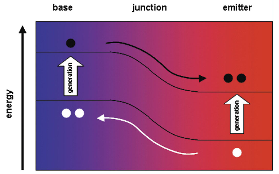
2. As soon as light is absorbed, electron-hole pairs are generated in both sides of the junction, with freed electrons moving up into the high energy conduction band, leaving behind holes in the valence band. This flow of electrons is sometimes called the generation current.
3. Next, electrons start to diffuse across the p-n junction from the p-type base layer down to the n-type emitter layer; the holes diffuse across the junction in the opposite direction. This diffusion is driven by the difference in energy levels between the emitter and base – a key point. The electrons (-ve) and holes (+ve) have opposite charge, so their movements in opposite directions reinforce each other. Note that the generation current continues to be driven by the ongoing absorption of photons.
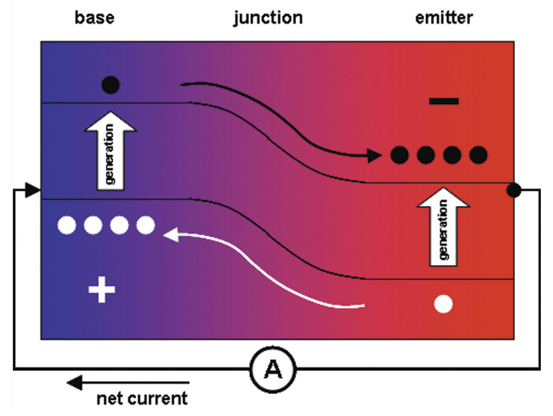
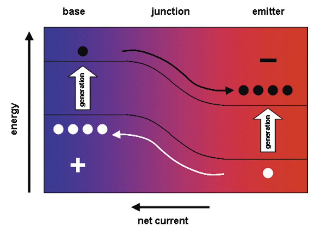
4. With the continued diffusion of electrons in one direction across the p-n junction, and holes in the other, a negative charge builds up in the emitter, and a positive charge in the base. The generation current between the bands has been transformed into an electrical current across the p-n junction.
5. If a circuit is connected between the contacts at the emitter and base sides of the solar cell, then a current will flow through this external circuit. Hook many of these circuits together in series and parallel as required, and you have effectively converted solar energy into usable electricity!


Share This Column